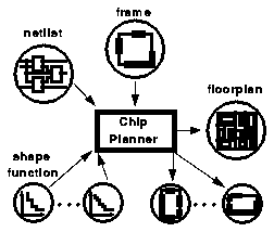
Input to a recursion step of the chip planner are the netlist and size/aspect ratio of the CUD (cell under design) as well as information about the area of the subcells. In the PLAYOUT system the latter data are given by the shape functions which have been computed by the shape function generator (SFG). The frame of the CUD further contains pin intervals, i. e. possible positions/intervals where nets can enter the cell. Output of the chip planner is a floorplan as `optimal' as possible as well as appropriate frames for the subcells.
Fig. 1.0.1: Input/Output of the Chip Planner
The chip planner computes the floorplan in two steps. The first step is placement, the determination of the topology, the second step is routing.
The aims of a (optimal) Placement are a total chip area which is as small as possible and short delay times. To reach this goal especially three subgoals must be reached:
The first task of the routing in the chip planner is the planning of the clock and power wiring of the circuit (clock and power routing), the second is the assignment of the nets of the netlist to the single channels between the cells (global routing). In that, course, length and need of area of the connection wires are computed.
The problems the chip planning has to solve are NP-complete. An efficient computation of the optimal solution is not possible because of the combinatorial variety. Therefore a suboptimal solution has to be found heuristically, that is near to the global optimum. Even then computation time and need of memory still increase very fast with the number of cells to be placed. The strongest restriction for the number of cells is given by the search for an appropriate global routing. The number of cells that can be placed in one step (i. e. the number of subcells per CUD) therefore should remain below an upper limit of 40 or 50.
The search for solutions near to the optimum leads to different chip planning strategies which consider the whole top-down process across the hierarchy levels. This is the topic of the last chapter.
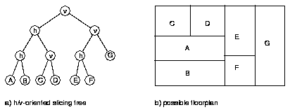
The structure of the tree resembles the neighbourhood relationship of the cells in the floorplan. Every inner node in the tree can uniquely be mapped to a slicing cut in the floorplan (and vice versa). Then the complete topology is defined by the orientation of the cuts and the relative order of two adjacent modules to a cut dividing them.
The fixing of floorplans to slicing structures is a limitation of cell placement possibilities. This limitation, though, will lead to worse results only in a few cases. On the other hand essential advantages for planning algorithms and in the chip assembly are gained by the slicing structure.
The oriented slicing tree is the result of the now described partitioning and placement steps.
The chip planner consists of three different partitioning algorithms: Cluster, Mincut and Inplace partitioning. A fourth method, Ratio-Cut partitioning, currently is implemented.
The Cluster algorithm works bottom-up, distributing the subcells to clusters and combining these cluster to even larger clusters until one big cluster is produced containing all subcells of the CUD. The heuristic of this algorithm consists in maximization of the connection costs inside a cluster.
The Mincut algorithm contrarily works top-down. It recursively divides the set of all cells into smaller partitions until such a partition only contains one cell. This heuristic minimizes the connection costs between the partitions (weight of the cut).
The Ratio-Cut algorithm essentially is an extension of the Mincut algorithm. The cost function of the Ratio-Cut partitioning not only considers the number of cut nets but also the balance of the partitions. Thus the Ratio-Cut partitioning tends to `natural' partitions, more than the Mincut heuristic for example. Here the heuristic is the minimization of the quotient of the cut weight and the product of the subtree sizes.
Every procedure computes the connection strength of cells and clusters resp. partitions (and thus an unoriented slicing tree), but the relative order of the cells remains undefined. This requires additional ordering steps. Because of its global sight in the first recursion steps the Mincut algorithm in most cases yields better results than the Cluster method. As already said the Ratio-Cut is still worked on.
The third algorithm performs an Inplace partitioning of the modules to be placed and generates a slicing tree in this manner. The word `inplace' describes the fact that this partitioning of a subset of modules considers the location of the CUD pins as well as the connections to modules that do not belong to the set to be partitioned. In order to consider the location of the CUD pins the designer has to define the orientation of the cuts on top level.
For the root node one point on the shape function is chosen (determination of the external frame of the CUD). For each point on the shape function it has been saved whether it is the result of vertical or horizontal addition of the sons. So the orientation of the cut (h/v-orientation) as well as the shape of both sons can be determined (sizing). The procedure is continued until the leafs are reached. The algorithm aims at determining the cuts of a given partitioning in a way that the area is as small as possible.
A special topic of sizing is the consideration of the wiring. The area
needed for the wiring of the subcells is estimated and partially added
to the area of the concerned subcells. This results in a shift (right
and up) of the shape function. As the nets are globally defined in the
net list, a net may connect cells of different hierarchy levels and so
may exist at severy hierarchy levels. For the purpose of estimation we
divide nets into segments that are fully contained in one level only.
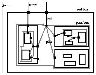
Here we use the following colour model:
Internal net segments, i. e. segments that are only connections between
subcells and do not leave the CUD, are displayed pink; red segments
are the connections to the frame of the CUD, i. e. to the external pins; the green
colour is assigned to the external wiring(cf. fig. 2.2.1). Depending on
which wiring area has been included we get shape functions for the
enclosing rectangles (pink, red and green box).
The additional wiring area is determined by the Track Demand method. Depending on the orientation of an edge cutting a net, track demands in orthogonal direction are necessary. A horizontal cut certainly causes a track demand in vertical direction, a vertical edge requires wiring area in X-direction. The quantity of the shift in X- and Y-direction is computed with the aid of statistically determined track demand factors which depend on the actual slice orientation.
The (topographic) l/r-ordering only examines a certain section (window) of the slicing tree at a time. The depth of the search window is configurable. Within the search window all possible arrangements of the modules are computed by mirroring the modules at the cuts. Call such an arrangement a configuration. The best configuration of a window is taken as the start orientation for the next (deeper) window.
The first objective of l/r-ordering is the minimization of the sum of net lengths over the configurations. Considering a given configuration, for each net a (heuristic) Steiner tree is build between the center of the modules the net connects (because the exact pin positions are not known yet).
To consider timing issues several approaches are workable:
After the determination of the geometrical ordering manual adjustments by exchange or movement of subcells can be performed. This interaction of designer and chip planner is supported by graphical output and extensive analysis. Since the chip planner essentially contains only heuristic algorithms this interaction (together with analysis) is a main part of chip planning.
As already said in chapter 2.3, normally the total net length is to be minimized (suitable cost parameters allow the inclusion of time critical nets). A first theoretical approach to routing problem therefore would be the search for a minimum spanning tree for the graph spanned by the vertices to be connected (cf. fig. 3.2.1 a). If the possibility exists to use further vertices besides the points to be connected and if we compute the the minimum spanning tree of this extended graph, we get a Steiner Tree whose total net length often is smaller (cf. fig. 3.2.1 b).
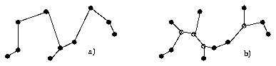
Fig. 3.2.1: Minimal Spanning Tree (a) and Steiner Tree (b)
Definition. Let G = (V,E) be a connected graph with vertex set V and edge set E.
Let λ : E > R+ be a cost function and R the subset of the required vertices of V.
A Steiner Tree is a subtree of G that connects all vertices in R and
all of whose leaves are vertices in R. A minimum Steiner Tree is a Steiner tree whose costs concerning λ are minimal.
For the global routing in the chip planner we use the following channel intersection graph model. Since the exact positions of the cell pins is not determined yet, the vertices to be wired (required vertices) are identified with the centres of theses cells. The edges essentially consist of the slicing lines of the (partitioned and oriented) floorplan. Additional vertices are the corners of the cells and the projections of the module centres to the slicing lines. Therefore, a net that connects the required vertices is a Steiner tree on this channel intersection graph (cf. fig. 3.2.2).
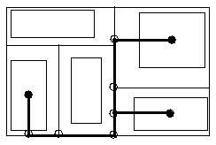
Fig. 3.2.2: Channel Intersection Graph with Steiner Tree
Now the chip planner performs the global routing sequentially. One net after the other is routed with the aid of Steiner tree heuristics, under consideration of restrictions given by the already routed nets. A heuristic method has to be used because the problem complexity - not at least because of the variable additional vertices - does not allow an exact computation.
The global routing assigns channels between the cells (resp. through the cells) to the nets. Course, length and need of area of the connecting wires are computed. The channel area is added to the adjacent cells proportionally. Since the sizes of the subcells change by this another sizing step must follow. The phases global routing and sizing have to be repeated as long as major changes in topography take place.
There is the dilemma that the computations of the shortest routes are always based on the old channels and new routes imply new channels again. Furthermore it cannot be guaranteed that after any number of iterations the total area converges at a minimum. The designer himself/herself has to decide after which iteration he or she wants to accept the result. In practice it has turned out that the results normally are already satisfying after two or three iterations.
Before the the chip planner is used the sizes of the subcells were computed by an area estimation step. The result of the estimation is a shape function that represents the minimal area of a cell for all aspect ratios. It is obvious that the quality of a top-down design depends very much on the quality of the estimation phase. However, it is not possible to estimate the area of a cell exactly. All estimation methods have tolerances because they do not have all informations the synthesis tools will have. The analysis of many test designs has shown that even small changes in the shape or size of a (sub)cell may result area disadvantages. These differences between estimation and final layout make an improved top-down chip planning method necessary.
Simple top-down chip planning computes a floorplan based on the shape functions in one isolated step per cell and determines a frame for the subcells in the sizing substep . These frames are input to the planning of the subcells and then obliging. The procedure starts on top-level with the whole chip, afterwards the subcells on the next lower level can be processed analogously and independently. So the computation of the subtrees can be performed parallelly.
A problem is here the unique determination of the cell frame on the basis of an estimated shape function (additionally the determination of pin is problematic). If later realizations cannot fulfil the frame restrictions the chip assembly phase has to compensate by means of cell enlargement, normally resulting in dead area. Without going into detail concerning possible kinds of errors it can be said that extensive tests have shown the impossibility of area estimation with a deviation of less than 10 - 15%. In the worst-case it can be even greater. In most cases this is inacceptable. One possibility to react upon deviations in top-down chip planning is to return to the shape function estimation phase and to change estimation parameters to gain shape functions of better quality. This would be a design iteration step which should have been avoided. A second possibility is to use realizations (layouts) of critical cells (using macros or multi-macros instead of flexible cells). The giving up of flexibility leads to loss of design quality, too.
A solution is the try to balance the deviations across several hierarchy levels in several phases. This approach is pursued in the Three-Phase chip planning method as described in the following.
So, it is useful after computing a floorplan of the CUD to perform an adjustment planning step for the supercell before continuing the top-down planning process at the subcell level. The deviations at the current level can be compensated at the supercell level (cf. fig. 4.1.1).
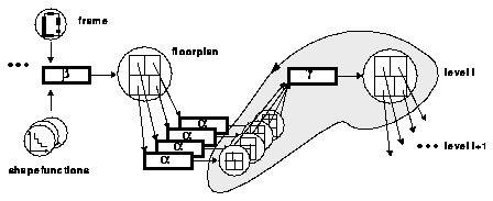
Fig. 4.1.1: Adjustment Process
There are three steps in the Three-Phase planning which we denote by greek letters ALPHA, BETA, and GAMMA. After planning the subcells at level i+1 (phase ALPHA), we perform an adjustment step at level i (phase GAMMA) before continuing the top-down planning of all subcells at level i+1 (phase BETA). Of course, the cell at level i itself is part of an adjustment process for its supercell on the level i-1. Thus, the three fundamental planning phases ALPHA, BETA, and GAMMA are performed with each cell except for those on top and bottom level. This gave the method its name.
In phase ALPHA we compute an initial floorplan whose topology will be fixed for all future planning steps. Since the subcells are still flexible many floorplans with different shapes but the same topology are feasible. We generate a refined shape function that describes all possible shapes of the same topology. This refined shape functions are more precise than shape functions of flexible cells because they rely on a particular topology and a global routing (not only on a rough wiring area estimation). They are input to the supercell adjustment (phase GAMMA).
Phase BETA adjusts the geometry of phase ALPHA to a new input frame. This frame stems from phase GAMMA of the supercell. After this phase the phase ALPHA of the subcell level can start.
Phase GAMMA is used for an adjustment to more precise subcell informations which are given by refined shape functions and computes a new frame for each cell.
In fig. 4.1.2 the process of Three-Phase chip planning on several hierarchy levels is shown in an abstract notation. In fig. 4.1.3 you see the data flow during the three phases. Not drawn is a floorplan which is also passed from ALPHA to BETA and from BETA to GAMMA.
Although there are bottom-up movements, the general direction of the process is top-down.
Fig. 4.1.2: Process of Three-Phase Chip Planning
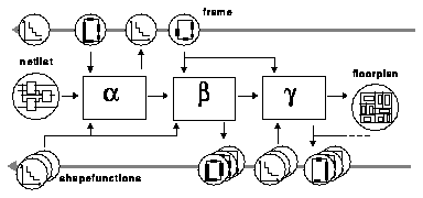
Fig. 4.1.3: Data Flow in the Three-Phase Chip Planning
In the meaning of stepwise refinement extensions of this method are possible, e. g. splitting of phase GAMMA into several adjustment phases or the inclusion of more levels. Thus the procedure becomes more and more complex and eventually you have to weigh up speed and quality of the design process. It must be considered further that increasing vertical and horizontal dependencies of the phases decrease the possibilities of parallelization.
Mirror sites:


