Therefore chip design is organized hierarchically. In principle there are two methods: the bottom-up and the top-down approaches. Early available commercial design systems were members of the first class. The bottom-up approach starts in designing the layout of a few base cells (small functional units, e. g. unique gates) with minimal area and minimal net length and in composing them to form larger cells. These cell clusters will again be composed and connected, resulting in even larger cells. This iteration continues until the whole chip is laid out. One disadvantage of this approach is that shapes of the individual cells normally produce dead area during the composition. This is especially the case if placement of cells, which themselves rarely fit together exactly, must meet demands on net lengths and delays. Dead area increases as complexity increases, and so the results of hierarchical design with several levels become worse. A second disadvantage is that the system cannot early tell the designer, if design meets requirements concerning area and clock rates, until the last iteration step (complete chip layout) is done. So possibly a great part of the process must be repeated.
Current state-of-the-art and future technologies require design systems that can handle several hierarchy levels efficiently and additionally can give early estimates about cell areas and delay times. This allows for checking specifications during the whole design process. These facilities can be provided by top-down oriented design systems like PLAYOUT.
Top-down design systems place the cells onto the chip by planning the shapes with a floorplanning tool. In the next step the shapes of the subcells of previously planned cells are computed, and so on. To generate a good floorplan it is profitable to have the layouts of the subcells to be workable. The easiest way to keep this are cells that are not laid out yet (flexible cells); if the layouts of some cells are designed already (macro cell library) they should be available in several shapes and with several timing characteristics to provide flexibility to a great extent.
The design is hierarchically performed from the chip area down to the level where the cells can be designed by a synthesis tool or manually. A main task is the estimation of subcell areas and timing behaviour. In the PLAYOUT system the sizes of the cells are being estimated by shape functions and the timing behaviour by timing graphs. This efficiently computable and early (in the design process) available functions provide some information about the needed area before any placement step has been done. As this top-down approach essentially consists of estimations we call this phase of the design process chip planning. A bottom-up assembly step follows. In this step the final layout is synthesized starting with the base cells, i. e. analogously to the bottom-up design but according to the floorplan, which has been computed top-down.
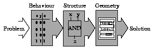
Orthogonally to the top-down division of the chip area many design systems divide the design process into several domains. At the beginning a description of the behaviour of the cell under design is created. The function of the chip can be given in form of a function table, an algorithmic description or in another mathematically unique form. Out of this behavioural description the layout is generated in several steps. First, a wiring diagram (structural description) is generated, whose components will be placed onto the available chip area (floor planning) and mapped into the geometric structures of the layout (mask layout).
Besides the synthesizing tools a design system needs validating components. These components compare the results a the design step with its specification (restrictions). Possible restrictions in the context of chip design concern a cell's need of area, the number of external connectors or the reachable performance (maximum clock rate). The validation can be performed by analysis, simulation, tests or verification. If discrepancies between realization and specification exceed a tolerable extent iterations of design become necessary, the avoidance of which is a main purpose of the top-down design approach, as explained above.
The subject of the next paragraphs is the systematic, hierarchical division of the design process into domains and abstraction levels.
Fig. 1.2.1: Domains (Threefold Division)
Especially in connection with top-down working design systems that do a floorplanning prior to the generation of the mask layout it has been useful to split the domain geometry into the two subdomains floorplanning and mask layout (cf. fig. 1.2.2).
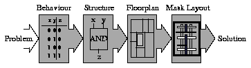
Fig. 1.2.2: Domains (Fourfold Division)
The problem dealt with is a chip which is to be designed with specified behaviour. First, a matching structure description is generated out of a (mathematically unique) behaviour description (structure synthesis). The structure description can be a wiring diagram or a module and net list. You can call it different views on the same domain.
The generation of a structure description from a behaviour description is not unique, because mostly there are several alternatives; for example a full adder can be realized by a ripple-carry adder or a carry-look-ahead adder. Special restrictions (e.g. area or timing behaviour) sometimes lead to different implementations.
To every alternative among the structure descriptions the following design step may generate one or more floorplans (chip planning). A floorplan maps every component of a circuit to its sub-area on the chip. In varying placements of the components the shapes and sizes of the alternative floorplans can turn out quite differently. The decision in favour of a special alternative is made in a compromise between minimal total area and connectability with short nets.
For every sub-circuit one or more layouts can be produced according to their structure and floorplan descriptions (cell synthesis), but the great expense and the narrow boundaries of the floorplan are the cause that normally only one alternative is looked at. A last design step is the composition and connection of the layouts of all sub-circuits according to the floorplan (chip assembly).
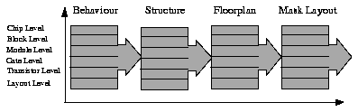
Fig. 1.3.1: Abstraction Levels
The objects of chip design are called cells. Domains and abstraction levels span a design plane (cf. fig. 1.3.1). The descriptions of cells at the cross points of abstraction levels and domains are called views. It is not necessary to have different views on cells of different abstraction levels or to have exactly one view on a cell at each cross point. The demand for data abstraction rather forces us to have the possibility of densed and structured descriptions of a cell. Densed descriptions take the place where a cell is a subcell of another one.
In the domain behaviour the function of a circuit is defined hierarchically (mostly top-down). In a first structure synthesis step this functional hierarchy may be mapped into a hierarchical wiring diagram (domain structure), which hierarchy borders agree with those of the behavioural description. The elements therefore are assigned to the individual hierarchy levels only according to functional point of view, without respecting geometric aspects, e. g. size and number of the cells on one hierarchy level. Thus an adaption to the requirements of physical design is necessary. Considering the cell under design (CUD), the structure synthesis provides a structure description of the CUD in form of a module list and a net list. The module list specifies the uses subcells, the net list the connections between them. If this cell appears as a subcell of another cell (supercell) this structured description is replaced by a densed one, namely the description of the external connectors.
This hierarchy of CUD, subcells and supercells (each sub- or supercell being the actual CUD may have its own subcells resp. supercells in turn) normally does not change any more in the following domains floorplan and mask layout (invariance of structure). The cell hierarchy in the floorplan is illustrated by fig. 1.3.2.

Fig. 1.3.2: Floorplan with Three Hi1:23 PM 3/27/2005erarchy Levels
The arrangement of the essential components of the PLAYOUT tools in the design plane is shown in fig. 2.0.1.

Fig. 2.0.1: Design Tools in PLAYOUT
The horizontal axis indicates the domains, the vertical axis the hierarchy levels. As PLAYOUT can handle a variable number of hierarchy levels many tools can be used in different levels. The dashed arrows in the figure give an example of the order in which the tools are applied in a simple design (one phase chip planning). A description of the individual tools follows.
A design data base provides module types of subcells to MIMOLA. If further components are generated by the synthesis their structure must be designed next, e. g. with the Schematic Entry or with a module generator. During the choice of subcells MIMOLA considers a cost factor (as a measure for the required chip area) as well as given delay times. The results of structure synthesis, i. e. module list and net list of the CUD, are converted into the PLIF data exchange language. This serves for communication with the design database.
Two things are worth to be mentioned about the conversion. First, 2-point nets with the same origin are combined to n-point nets. This is necessary because MIMOLA works only with 2-point nets. Further, level sensitive registers can be replaced by edge triggered registers.
The designer can dispose of components in form of type descriptions of standard cells (from a standard cell catalogue) as well as of already designed cells. If necessary, the standard cell library may be expanded with the help of a Layout Editor, which allows graphical entry of layout objects. The specified behaviour now must be realized with the help of these components. The type descriptions form a mechanism of data abstraction being applied in PLAYOUT.
So, some hierarchy levels contain too many cells (MIMOLA typically generates circuits with some hundreds of RT modules), surpassing a upper bound given by the complexity of the algorithms of the following chip planning phase. Other hierarchies are very deep, the individual levels consisting of only a few cells. Also this is not very useful as a certain least number must not be fallen short of because of some statistic assumptions. Furthermore, in typical, only functionally partitioned wiring diagrams large cells (e. g. memory blocks) often lie besides very small cells (e. g. inverters) on one hierarchy level.
The functional hierarchy therefore must be transformed into another hierarchical structure description, more suitable for the further geometric design. Such a transformation step, namely transformation of a structure description into a new hierarchy under consideration of all restrictions, is called repartitioning. It takes place in the domain structure.
The PLAYOUT tool for this is called repartitioner. During the computation of the most convenient partition of the CUD it considers several factors. As already mentioned, the physical design tools reach the best results if the number of cells to be worked on lies inside certain bounds and the sizes of the cells are well-balanced. The number of cut nets as well as the number of hierarchy levels influence the required chip area. The decision inside which partition a net is routed influences the timing behaviour of the circuit. To do the task the repartitioner needs a global view on the circuit including all hierarchy levels. It is provided by the design data base in form of a configuration tree. The result of this design step is another configuration tree describing the repartitioned structure.
As the SFG is working in the domain structure, it cannot know the geometric course of the nets. Therefore it computes statistical extra area for the routing and adds it to the area of the subcells. The latter themselves are described by shape functions, so this tool is applied bottom-up to chip level. In order to compute the shape functions the SFG does a recursive bipartitioning according to the Mincut method.
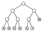
Fig. 2.4.2: Unoriented Slicing Tree
The result is an unoriented slicing tree (cf. fig. 2.4.2) whose leaves are the subcells. For each inner node the shape functions are added by the SFG according to the Optimal Superposition method (cf. fig. 2.4.3) and the more convenient orientation (horizontal or vertical) is saved.

Fig. 2.4.3: Optimal Superposition of Shape Functions
It has been shown that the shape functions of the SFG are not only efficiently computable but also provide a good estimation of the size of a cell, even if the following design step does not use the Mincut method. The SFG only must be given suitable parameters. The integration of delay time estimations has not been solved satisfactorily yet.
Here is a more detailed description of the Chip Planner.
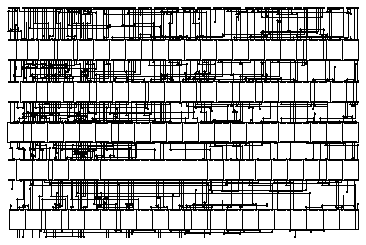
Fig. 2.6.1: Result of Standard Cell Placement with Simulated Annealing
The input of the chip synthesis is the floorplan of the CUD, the global routing and the frames of the subcells. The chip synthesis completes the mask layout by detailed routing. Detailed routing is the determination of the exact course of each net assigned to a channel. Prior to that, some compacting steps are performed, because normally the synthesized mask layout slightly differs from the estimated area. Afterwards the channels that may be used by detailed routing can be extracted. If the respective cells cannot be placed and routed inside the given frame some design steps must be iterated until the estimations lead to a realizable chip layout.
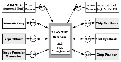
Fig. 2.8.1: Communication with the Design Database
Mirror sites:


